Why are more and more data centers using FPGAs?
1) Using FPGA design ASIC circuit (application-specific integrated circuit), users do not need to shoot production, you can get a shared chip.
2) The FPGA can be used as a mid-sample for other full-custom or semi-custom ASIC circuits.
3) The FPGA has a wealth of internal flip-flops and I/O pins.
4) FPGA is one of the devices with the shortest design cycle, lowest development cost, and lowest risk in ASIC circuits.
5) FPGA uses high-speed CMOS technology, low power consumption, compatible with CMOS and TTL levels.
Three advantages of FPGA Advantage 1: A greater degree of parallelismThis is mainly achieved through both concurrent and streaming technologies. A: Concurrency refers to the repeated allocation of computing resources so that multiple modules can perform calculations independently at the same time. This is similar to the current multi-core and SIMD technologies. But relative to SIMD technology, FPGA concurrency can be performed between different logic functions, not limited to performing the same function at the same time. A simple example is that using SIMD can perform multiple additions at the same time, while FPGA can perform multiple additions and multiplications at the same time and any logic you can design.
B: Streaming is performed by segmenting tasks and executing them at the same time. In fact, this is similar to the CPU, except that the CPU is running between instructions and the FPGA is running between tasks or can be said to be inter-threaded.
Advantage two: can be customizedFPGAs implement logic through LookupTable and can be simply understood as hardware circuits. Customizable means that users can implement their own logic circuits within the allowable range of resources. Under normal circumstances, the task running on the hardware circuit is faster than the software, for example, to compare the size of a 64-bit high 32-bit and low 32-bit, under the CPU requires two regions instructions, two bits and instructions, A shift instruction is a compare instruction and a writeback instruction, and only one comparator is required under the FPGA.
Advantage three: reconfigurableReconfigurable means that the logic inside the FPGA can be changed according to requirements, reducing development costs. At the same time, using FPGAs to reuse resources saves more space for the server than using multiple fixed ASIC modules.
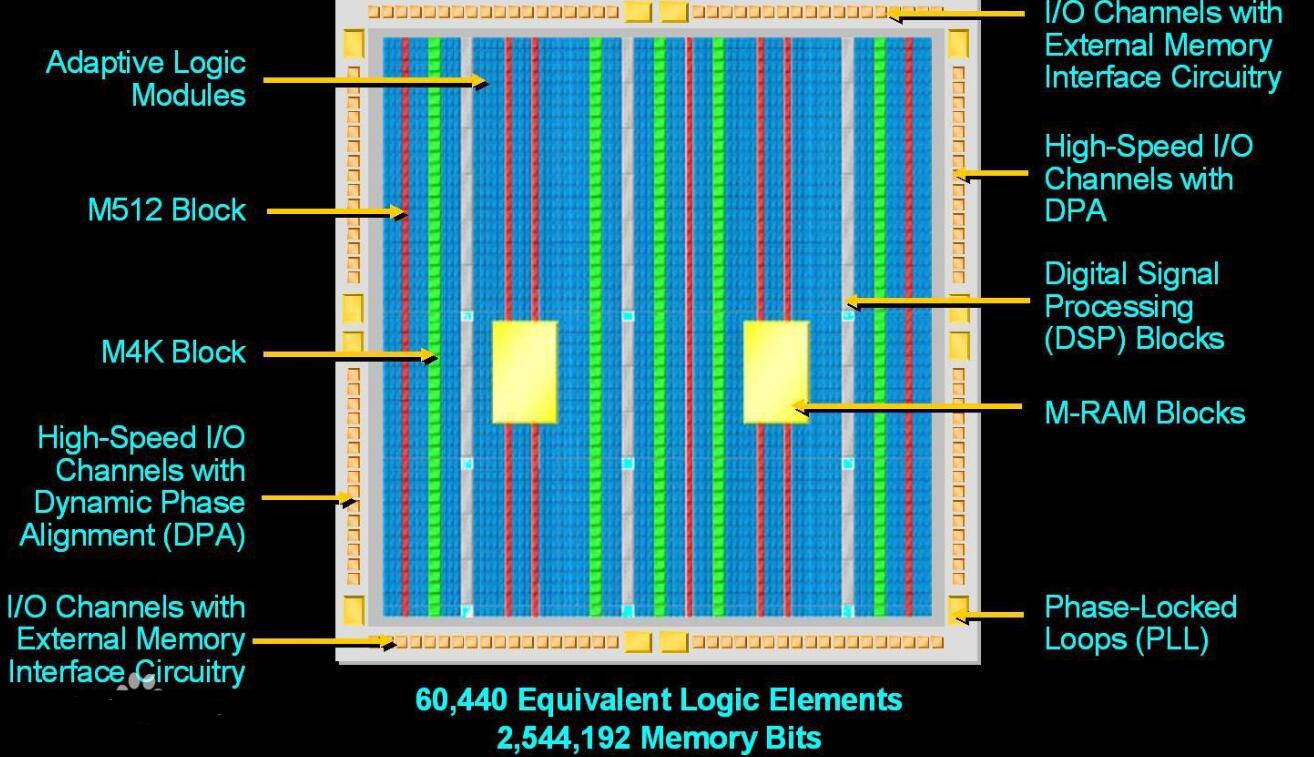
FPGA adopts the concept of logic cell array LCA (Logic Cell Array), including three parts: configurable logic block CLB (Configurable Logic Block), output input block (IOB) and internal interconnect (Interconnect). Field programmable gate arrays (FPGAs) are programmable devices that have a different structure than traditional logic circuits and gate arrays (such as PAL, GAL, and CPLD devices). The FPGA uses a small lookup table (16×1 RAM) to implement the combinatorial logic. Each lookup table is connected to the input of a D flip-flop. The flip-flop drives other logic circuits or drives the I/O. This makes it possible to implement a combination. Logical functions can also implement basic logic unit modules for sequential logic functions. These modules are connected to each other or to I/O modules using metal wires. FPGA logic is implemented by loading programming data into internal static memory cells. Values ​​stored in memory cells determine the logic functions of logic cells and the connection between modules or modules and I/O, and ultimately determine the FPGA can realize the function, FPGA allows infinite programming.
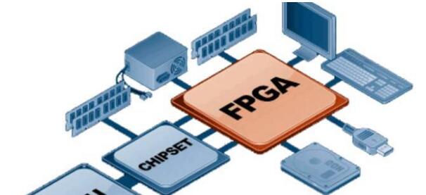
1. Application of FPGA in Data Acquisition
Since most signals in nature are analog signals, the general signal processing system must include the data acquisition function. A common implementation method is to use an A/D converter to convert an analog signal into a digital signal and then send it to a processor, such as an MCU or a digital signal processor (DSP) for operation and processing.
For low speed A/D and D/A converters, a standard SPI interface can be used to communicate with the MCU or DSP. However, high-speed A/D and D/A conversion chips, such as video decoders or encoders, cannot directly interface with general-purpose MCUs or DSPs. In this case, FPGA can complete the glue logic function of data acquisition.
2. Application of FPGA in Logic Interface Field
In actual product design, data communications with the PC are required in many cases. For example, the collected data is sent to the PC for processing, or the processed results are passed to the PC for display. The interface between the PC and the external system is relatively rich, such as ISA, PCI, PCI Express, PS/2, and USB.
Traditional design often requires a dedicated interface chip, such as a PCI interface chip. If more interfaces are needed, more peripheral chips are needed, and the size and power consumption are relatively large. With the FPGA solution, the interface logic can be implemented inside the FPGA, greatly simplifying the design of the peripheral circuit.
In modern electronic product design, memory has been widely used, such as SDRAM, SRAM, Flash and so on. Each of these memories has its own characteristics and uses. Reasonable choice of memory type can achieve the best price/performance ratio of the product. Because the functions of the FPGA can be completely designed, it is possible to implement controllers for various memory interfaces.
3. Application of FPGA in Level Interface Field
In addition to TTL and COMS interface levels, new level standards such as LVDS, HSTL, GTL/GTL+, and SSTL are gradually being adopted by many electronic products. For example, the LCD driver interface is generally an LVDS interface, the digital I/O is generally an LVTTL level, and the DDRSDRAM level is generally an HSTL.
In such a mixed-level environment, if the interface is implemented with a conventional level-shifting device, the circuit complexity will increase. Using FPGAs to support multi-level coexistence features can greatly simplify design and reduce design risk.
Second, high-performance digital signal processingWireless communications, software radios, high-definition video editing and processing, etc., place very high demands on the amount of computation required for signal processing. Traditional solutions generally use multiple DSPs in parallel to form a multiprocessor system to meet the needs.
However, the main problem brought by multi-processor systems is that the design complexity and system power consumption are greatly increased, and the system stability is affected. FPGAs support parallel computing, and their density and performance are constantly improving, and traditional multi-DSP solutions can already be replaced in many areas.
For example, an HD video encoding algorithm H.264 is implemented. Using TI's 1GHz clocked DSP chip requires four chips, and the use of Altera's StratixIIEP2S130 chip requires only one to complete the same task. The implementation flow of the FPGA is similar to the front-end design of the ASIC chip, which is conducive to the introduction of the back-end design of the chip.
Third, other application areasIn addition to the above application areas, FPGAs also have a wide range of applications in other fields.
(1) Automotive electronics, such as gateway controllers/car PCs, and telematics systems.
(2) Military areas such as security communications, radar and sonar, and electronic warfare.
(3) Test and measurement areas such as communications testing and monitoring, semiconductor automated test equipment, and general-purpose meters.
(4) Consumer products, such as monitors, projectors, digital TVs, set-top boxes, and home networks.
(5) Medical fields such as software radio, electrotherapy, and life sciences.
Why do data centers use FPGAs?As we all know, the Moore's Law for general-purpose processors (CPUs) has entered the leap year, while the scale of machine learning and Web services has grown exponentially. People use custom hardware to speed up common computing tasks, but the ever-changing industry demands that these customized hardware be reprogrammed to perform new types of computing tasks.
FPGA (Field Programmable Gate Array) is a kind of hardware reconfigurable architecture. It has been used as a small-batch replacement for ASICs for many years. However, in recent years, data centers in Microsoft, Baidu and other companies have been deployed on a large scale to simultaneously Provides powerful computing power and sufficient flexibility.
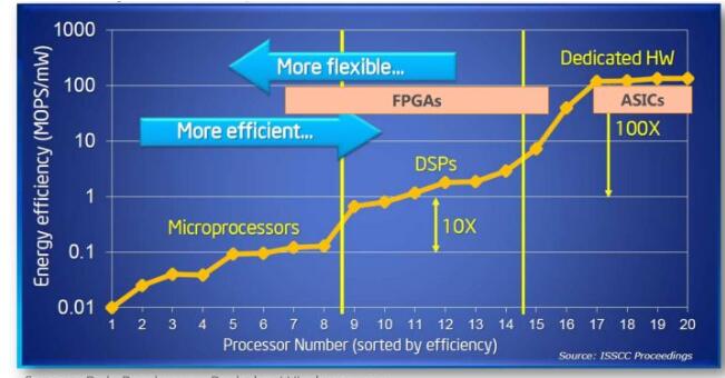
Why is FPGA faster? "It's all set off by colleagues." The CPU and GPU all belong to the von Neumann structure, and the instruction decode execution and shared memory. FPGAs are more energy efficient than CPUs or even GPUs, and are essentially the benefits of an instructionless, shared-nothing architecture.
In the Feng's architecture, since an execution unit (such as a CPU core) may execute any instruction, it needs an instruction memory, a decoder, various instruction operators, and branch jump processing logic. Due to the complex control logic of the instruction stream, there may not be many independent instruction streams. Therefore, the GPU uses SIMD (single instruction stream multiple data stream) to allow multiple execution units to process different data at the same pace. The CPU also supports SIMD. instruction. The function of each logic cell of the FPGA is already determined during reprogramming (programming) and no instructions are required.
The use of memory in the Feng structure has two roles. One is to save the state and the other is to communicate between execution units. Since memory is shared, access arbitration is required; in order to utilize access locality, each execution unit has a private cache, which is to maintain the consistency of the cache between execution components. For the preservation of state requirements, the registers and on-chip memory (BRAM) in the FPGA are part of their respective control logic and do not require unnecessary arbitration and caching. For communication needs, the connection between each logic cell of the FPGA and the surrounding logic cells is determined at the time of reprogramming (programming) and does not require communication through shared memory.
With so many 3,000 feet tall, how does the FPGA actually perform? We look at compute-intensive tasks and communication-intensive tasks, respectively.
Examples of computationally intensive tasks include matrix operations, image processing, machine learning, compression, asymmetric encryption, Bing search ordering, and the like. This kind of task is generally the CPU offloads the task to the FPGA. For this type of task, we are currently using Altera (should seem to be called Intel, I still used to call Altera ...) StratixVFPGA integer multiplication performance and 20-core CPU is basically equivalent, floating-point multiplication performance and 8-core CPU It's basically the same, but an order of magnitude lower than the GPU. We are about to use the next-generation FPGA, Stratix10, will be equipped with more multipliers and hardware floating-point components, so that theoretically it can achieve the computing power comparable to the current top GPU computing cards.
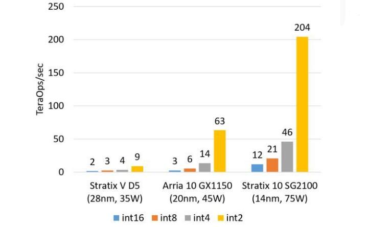
FPGA's integer multiplication ability (estimated value, without DSP, estimated based on logical resource occupancy)
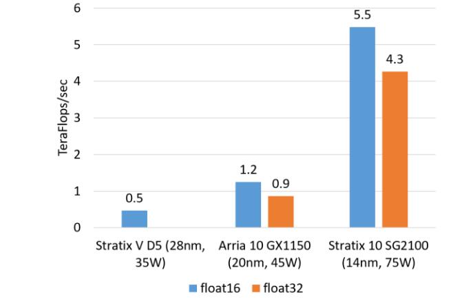
FPGA floating-point multiplication capability (estimated value, soft16 for float16, hardcore for float32)
In data centers, the core advantage of FPGAs over GPUs is latency. Tasks such as Bing search sorting, to return search results as quickly as possible, need to reduce the delay of each step as much as possible. If you use a GPU for acceleration, to make full use of the GPU's computing power, the batch size cannot be too small, and the delay will be in the order of milliseconds. With FPGA acceleration, only microsecond PCIe latency is required (our current FPGA is a PCIe accelerator card). After Intel introduced the Xeon+ FPGA connected through QPI in the future, the delay between the CPU and the FPGA can be reduced to less than 100 nanoseconds, which is no different from accessing the main memory.
Why is FPGA less latency than GPU? This is essentially the difference in architecture. FPGAs have both pipeline parallelism and data parallelism, while GPUs have almost only data parallelism (pipeline depth limited). For example, there are 10 steps to process a data packet. The FPGA can build a 10-stage pipeline. Different stages of the pipeline process different data packets. Each data packet flows through 10 levels and is processed. Each processing completes one data packet and can be output immediately. The GPU data parallel method is to do 10 calculation units, each computing unit is also dealing with different data packets, but all computing units must do the same thing at the same pace (SIMD, SingleInstructionMultipleData). This requires that 10 packets must be input together and output together, and the delay of input and output increases. Pipeline parallelism achieves lower latency than data parallelism when the tasks are arriving on a one-by-one basis rather than in batches. As a result, FPGAs inherently have latency advantages over GPUs for streaming computations.
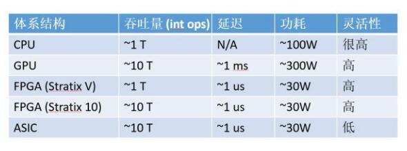
Computationally intensive tasks, magnitude comparisons of CPUs, GPUs, FPGAs, and ASICs (taking a 16-bit integer multiplication as an example, numbers are only magnitude-level estimates
ASIC-specific chips are blameless in terms of throughput, latency, and power consumption, but Microsoft has not adopted them for two reasons:
The computational tasks of the data center are flexible, and the ASIC development costs are high and the cycle is long. It was finally difficult to deploy a large number of acceleration cards for certain neural networks on a large scale. As a result, another type of neural network became even hotter and the money was wasted. FPGAs can update logic functions in just a few hundred milliseconds. The flexibility of FPGAs can protect the investment. In fact, Microsoft's current FPGA gameplay is very different from the initial scenario.
The data center is leased to different tenants for use. If some machines have a neural network accelerator card, some machines have a Bing search accelerator card, some machines have a network virtualization accelerator card, the scheduling of tasks and the transport of servers. Victoria will be very troublesome. Using FPGAs can maintain the homogeneity of the data center.
Next look at communication-intensive tasks. Compared with computationally intensive tasks, communication-intensive tasks do not deal with the processing of each input data. They are basically simply calculated and output. At this time, communication often becomes a bottleneck. Symmetric encryption, firewalls, and network virtualization are all examples of communication-intensive.
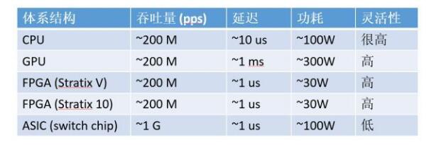
Communication-intensive tasks, order-of-magnitude comparison of CPUs, GPUs, FPGAs, and ASICs (using 64-byte network packet processing as an example, numbers are only estimates of magnitude)
For communications-intensive tasks, FPGAs have greater advantages over CPUs and GPUs. From the throughput point of view, the transceiver on the FPGA can be directly connected to the 40Gbps or even 100Gbps network cable, to process any size packet at wire speed; and the CPU needs to receive data packets from the network card to handle, many network cards can not be wire speed Handle 64 bytes of small packets. Although it is possible to achieve high performance by inserting multiple network cards, the number of PCIe slots supported by CPUs and motherboards is often limited, and the network cards and switches themselves are expensive.
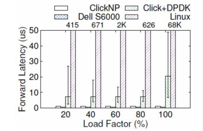
In terms of delay, the network card receives the data packet from the CPU and the CPU sends it back to the network card. Even if a high-performance packet processing framework such as the DPDK is used, the delay is 4 to 5 microseconds. The more serious problem is that the delay of general-purpose CPU is not stable enough. For example, when the load is high, the forwarding delay may rise to tens of microseconds or even higher (as shown in the figure below); clock interruption and task scheduling in modern operating systems also increase the uncertainty of the delay.
Although the GPU can also process packets with high performance, the GPU does not have a network port, which means that you need to first receive the packets from the network card and let the GPU do the processing. This throughput is limited by the CPU and/or network card. Not to mention the delay of the GPU itself.
So why not put these network functions into network cards or use programmable switches? The flexibility of the ASIC is still flawed. Although there are more and more powerful programmable switches, such as Tofino, which supports the P4 language, ASICs cannot perform complex stateful processing, such as some kind of custom encryption algorithm.
In summary, the main advantages of FPGAs in data centers are stable and extremely low latency, suitable for streaming computationally intensive tasks and communication-intensive tasks.
Multi-Port Hub2.0,Power Bank Charger,Wireless Charging Stations,Universal Laptop Charger
shenzhen ns-idae technology co.,ltd , https://www.szbestchargers.com
