
The application of the defect structure in the mutual coupling suppression between microstrip antennas is explained in detail.
Microstrip antennas are widely used in various communication systems as well as radar, telemetry, navigation, and biomedical fields because of their unique advantages over other antennas. With the development of information technology, it is necessary to research and develop microstrip antennas and arrays with better performance. In order to obtain high gain and obtain properties such as beam scanning or beam steering, it is necessary to form discrete antenna elements into an array. In an array environment, there is energy coupling between the antenna elements, which degrades the performance of the antenna. Usually the mutual coupling between microstrip patches is caused by both spatial and surface waves. Studies have shown that when the dielectric substrate thickness of the antenna is small, the inter-cell coupling is mainly performed by spatial waves, and the influence of surface waves is negligible. For thicker substrates, the effect of surface waves will increase. The thicker the dielectric substrate, the more surface modes the excitation will have, and more power will be coupled into multiple modes of excitation. When the spacing between the two antenna elements exceeds a certain value, the coupling of the surface waves begins to dominate. The existence of mutual coupling effects will affect the antenna pattern, input impedance and gain of the array, which must be considered in the design of the antenna array.
In order to reduce the mutual coupling between the antenna elements, a photonic bandgap structure is employed. This structure either etches holes in the floor or perforates the medium to form a frequency stop band for the surface wave propagation mode, thereby suppressing surface waves and reducing coupling. Although this method can improve the radiation efficiency of the antenna, the periodic punching in the medium is troublesome in the manufacturing process, and a large number of etching periodic patterns on the floor will result in limitation of the placement of the antenna. The bandgap property of the electromagnetic bandgap material (EBG) is used to suppress the propagation of the surface wave and reduce the mutual coupling of the antenna. The EBG structure is composed of an array of several units, so the structural analysis is complicated.
Similar to the PBG structure, the DGS structure also changes the distribution of the effective dielectric constant of the circuit substrate material by etching a defect pattern on the ground plane of the circuit, thereby changing the distributed inductance of the microstrip line based on the medium. And distributed capacitance, which makes such microstrip lines have bandgap characteristics and slow-wave characteristics, and has the advantages of simple fabrication, small size, and easy integration. The advantage of the DGS structure compared to the EBG (PBG) structure is that resonance can be generated at certain frequency points without establishing a periodic structure, providing good bandgap characteristics and can be characterized by a simple LC equivalent circuit model. Fast circuit level analysis is available. DGS structure is more competitive than EBG (PBG) structure in terms of equivalent process conditions and performance requirements, in the integrated circuit industry, which is sensitive to economic cost changes considering circuit size, and the current miniaturization of wireless communication equipment. force. At present, the structure has been widely used in the design of discrete components of microwave circuits, such as microstrip lines, filters, resonators, amplifiers, oscillators, antennas, and the like.
However, as far as the author is aware, few studies have examined the role of DGS in the mutual coupling between array antenna elements. In this paper, Ansoft HFSS simulation software is used to analyze the frequency characteristics of DGS. The electromagnetic field simulation results and Ansoft Designer's circuit simulation results are used to extract the parameters of the equivalent circuit, and the effect of the defect structure on the mutual coupling between the array antenna elements and the antenna performance is studied. . In order to fully explain the influence of DGS structure on antenna performance parameters, the performance parameters of common patch antenna arrays with the same structure size are also given, and the two are compared.
2 DGS structure and its band gap characteristicsIn this paper, a DGS structure with a stopband center frequency of about 6.5 GHz is designed. The circuit uses a dielectric substrate with a relative dielectric constant of 10.2 and a thickness of 2 mm. The microstrip line is an ordinary 50 Ω impedance line with a width of 3 mm. The DGS structure consists of two back-to-back U-shaped grooves, as shown in Figure 1. The structural parameters of DGS are l1=3.3mm, w1=7.4mm, g=4.5mm, s=1.5mm. The etched single U-shaped slot can be equivalent to an LC parallel circuit, as shown in Figure 2. Changing the parameters of the DGS will also change its frequency characteristics and equivalent LC parameter values.
In this paper, Ansoft HFSS is used to simulate the transmission characteristics of microstrip lines. The simulation results are shown in Figure 3. The results show that the DGS microstrip transmission line has a wide stopband characteristic, the loss from 5.64GHz to 7.26GHz is greater than 20dB, and the lowest point in the band is 38.6dB.
The frequency characteristic of the DGS unit is similar to that of the two-pole Butterworth low-band rejection filter, and can be determined by its 3dB cutoff frequency and resonant frequency. Therefore, by making the equivalent impedance of the LC parallel connection equal to the impedance of the two-pole Butterworth band rejection filter, the inductance value and capacitance value of the LC parallel circuit can be obtained. The DGS equivalent circuit parameter values ​​extracted from the simulation results are: L1=1.682nH, C1=0.400pF, L2=1.747nH, and C2=0.321pF. Figure 3 is a comparison of the 3D field simulation results of the DGS unit with its equivalent LC circuit simulation results. The simulation results show that the frequency characteristics of the two are basically the same, and the DGS unit can be equivalent to the LC parallel circuit.
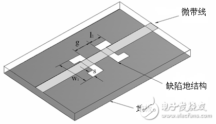
Figure 1 DGS microstrip line schematic
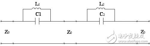
Figure 2 DGS microstrip line equivalent circuit diagram
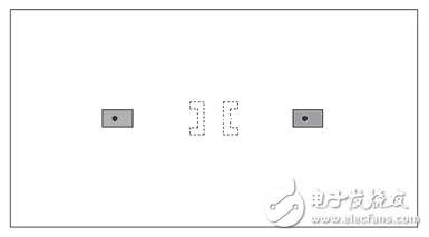
3 Microstrip array antenna design and analysisThe high dielectric constant helps to reduce the size of the antenna unit, while increasing the thickness of the medium can broaden the bandwidth. However, this also exacerbates the excitation of the surface waves, resulting in strong coupling such that the antenna performance is degraded. The influence of dielectric constant and dielectric thickness on the coupling between microstrip antenna elements is studied in [10]. Studies have shown that when the substrate is thick, the mutual coupling of the E-plane of the microstrip antenna element is stronger when the dielectric constant is large, and the mutual coupling of the H-plane is stronger when the dielectric constant is relatively small. Here we select a substrate with a dielectric constant of 10.2 and a substrate thickness of 2 mm. At this time, the mutual coupling of the E faces is significantly stronger than the mutual coupling of the H faces. We have designed a binary array with E-plane coupling using coaxial feed, as shown in Figure 4. The size of the microstrip antenna unit is 6.8 mm & TImes; 4 mm, and the distance between the two antenna elements is 36.9 mm (0.75 lg).
In order to reduce the coupling of the E-plane, we introduce a DGS structure between the array elements. When the radiation frequency of the antenna falls exactly in the band-stop frequency band of the DGS, the surface wave is suppressed, thereby reducing the coupling between the array elements.
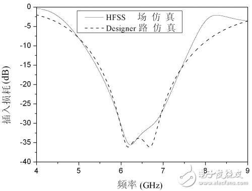
Figure 3 Simulation results of the DGS unit
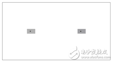
(a)
(b)
Figure 4 Binary antenna array structure diagram (a) Top view (b) Back view
We calculated and tested the insertion loss and return loss for both the DGS structure and the DGS structure, as shown in Figure 5 and Figure 6. The normal patch antenna array with no DGS structure on the substrate has an operating frequency of f 0 = 6.04 GHz. After the DGS structure is introduced, the operating frequency of the antenna is hardly shifted, which indicates that the DGS has little influence on the resonant frequency of the antenna. It can be seen from the S21 parameter that the coupling between the antennas is significantly reduced after the introduction of the DGS structure between the antenna elements E. At the operating frequency, the coupling between the antenna elements is reduced from -16.9dB in the absence of the DGS structure to -25.9dB in the DGS structure, which is reduced by 9dB.
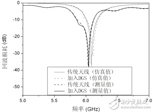
Figure 5 Simulation and test return loss
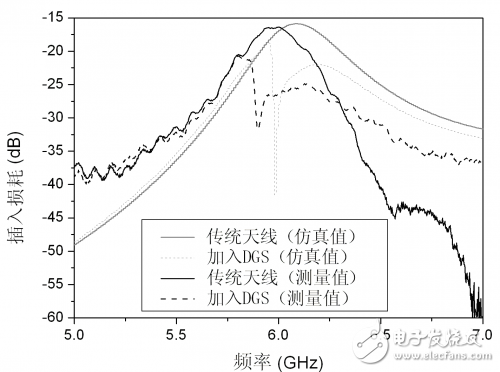
Figure 6 Simulation and test insertion loss
This shows that the DGS structure can effectively weaken the coupling between the array elements.
To further see the effect of DGS on the far-field radiation characteristics of the antenna, Figure 7 compares the E-plane radiation pattern of the array antennas of two different structures at the resonant frequency. It can be seen that the improvement of the E-plane pattern is obvious, the whole beam is more closed, the relative value of the first sidelobe level is reduced by 3 dB, and the gain increase is not very obvious, which is increased by about 1 dB. It can be seen that the DGS structure can reduce the coupling between the antenna elements, reduce the sidelobe level, and improve the gain of the antenna, thereby improving the radiation performance of the antenna array.
4 ConclusionThis paper focuses on the band-stop characteristics of a DGS structure and its effect on the microstrip antenna array. It was applied to a microstrip patch array and compared to a microstrip antenna array without DGS structure. The result analysis shows that the DGS structure can significantly reduce the coupling between the antenna elements, increase the gain of the antenna, and significantly improve the antenna performance.
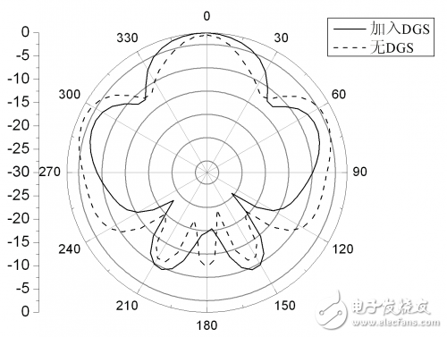
Figure 7 E-plane simulation direction
This simple DGS structure has a good application prospect in the design of suppressing the coupling between antenna array elements.
With 15+ years manufacturing experience for Portable Power.
Supply various portable charger for iPhone, Airpods, laptop, radio-controlled aircraft ,laptop, car and medical device mobile device, ect.
From the original ordinary portable power source to Wireless Power Bank, Green Energy Solar Power Bank, Magnetic Mobile Power, Portable Power Stations and other products continue to innovate.
Avoiding your devices run out of charge, Portable Chargers to keep your mobile device going.
We help 200+ customers create a custom mobile power bank design for various industries.
Wireless Earphones,Wireless Headphones,Best Wireless Headphones,Best Bluetooth Earphones
TOPNOTCH INTERNATIONAL GROUP LIMITED , https://www.micbluetooth.com